

Custom Search
|
|

|
||
 MIL-HDBK-419A
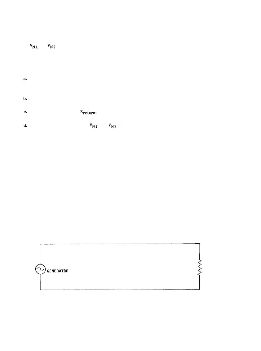
An ideal signal system is a simple signal generator-load pair as shown in Figure 6-1. With no extraneous
voltages present within the loop, this simple pair is free of interference. Consider, however, what happens
when the current return path is non-ideal and sources of noise are present as shown in Figure 6-2. Unless noise
voltages
and
are identical, a voltage difference will exist between the low side of the generator (Node
1) and the low side of the load (Node 2). As shown in Figure 6-3, this voltage difference effectively appears in
the signal transfer loop in series with the signal generator and produces noise currents in the load. Four ways of
combating this noise problem are as follows:
Isolate the source-load pair from the noise sources; i.e., float the system and provide the necessary
shielding and filtering to prevent coupling by other means.
Connect the low side of the loop to the reference plane at either Node 1 or Node 2 but not at both.
Reduce the impedance,
of the path connecting the two noise sources.
Reduce the magnitudes of
and
through the control of the currents producing them by
lowering the impedance through which these currents flow.
Practical electronics circuits typically are a collection of several source-load combinations such as shown in
Figure 6-4. These various source-load combinations may be functionally dependent on each other. Hence each
individual source-load pair can not operate in isolation, there must be coupling between pairs. For example, one
source may be driving several loads; one load may be receiving signals from several sources; or the load for one
signal source may serve as the source for another load. At the circuit level, numerous sources and loads are
connected in an interrelated fashion and the use of individual return paths for each source-load pair becomes
impractical. It is more realistic to establish a common ground or reference plane which serves as the return
path for several signals. The control of undesired network responses, particularly in high gain and/or higher
frequency circuits, often requires the establishment of a common signal reference to which functional grouping
of components, circuits, and networks can be connected. Ideally, this common reference connection offers zero
impedance paths to all signals for which it serves as a reference. The several signal currents within the
network can then return to their sources without creating unwanted conductive coupling between circuits.
LOAD
Figure 6-1. Idealized Energy Transfer Loop
6-2
|
 
|
|
|
||


